

Excited-State Dynamics in Organic Semiconductors, Nanocrystals, and Metal-organic Frameworks
 |
|
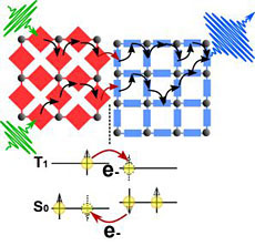
Figure 1: Schematic of the processes of photon upconversion by triplet annihilation in a bilayer stack of surface-anchored metal-organic frameworks. |
We are interested in understanding and controlling the motion of excited states within novel semiconductors, be it charge-carrier hopping away from an exciton-splitting interface in an organic solar cell or the motion of triplet excitons within crystalline metal-organic frameworks. Gaining an understanding of how excited-states move in nanoscale spatial dimensions on ultrafast timescales allows us to establish the consequences of nanoscale and molecular design on the macroscopic functional performance of a material.
Our recent work on establishing the behavior of charge-transfer states at organic semiconductor interfaces can be found in the Journal of Physical Chemistry C (1,2); and our work on creating surface-anchored metal-organic framework heterojunctions that control triplet transport to allow photon upconversion can be found in Advanced Materials.
Dipolar Molecular Rotors in SURMOFs
 |
|
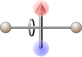
Figure 1: Schematic of a dipolar rotor whose stator can be integrated into a surface-anchored metal-organic framework. The grey spheres indicate reactive units that bind the stator into the crystalline structure. The dipolar fragment of the molecule (indicated by the arrow) can then rotate freely around this stator. |
As part of the DFG Priority Program 1928 “Coordination Networks: Building Blocks for Functional Systems”, we are investigating the dynamics of strongly interacting dipolar molecular rotors in collaboration with Prof. Herges at the Christian-Albrechts-Universität zu Kiel and Dr. Xianghui Xhang at Universität Bielefeld. We are developing materials that incorporate the dipolar molecular rotors into the building blocks of crystalline surface-anchored metal-organic frameworks; this allows the dipolar-dipolar interactions to be tuned in three dimensions and low-energy macroscopic orderings to be designed. By integrating these films into device structures, we hope to demonstrate field-induced switching of the dipolar rotor macroscopic orientation patterns and move towards realizing a new material concept for fast optical switching.
Further information can be found on the Priority Program’s website.
 |
|
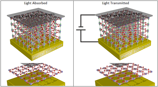
Figure 2: Showing a dipolar-rotor-based SURMOF light modulation device. Without applied field (left), the permanent and transition dipole moments (red arrows) lie in a collective low energy configuration in the substrate plane giving the device a high optical absorption. When bias is applied, the dipoles are rotated into a configuration with the dipoles perpendicular to the substrate plane giving the device a low optical absorption. The bottom row illustrates a zoomed view of the dipole alignment. For our prototype device we will use a (semi)-transparent gold bottom contact and graphene top contact. |
Stimulated Emission and Lasing in Perovskites
 |
|
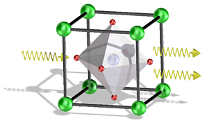
Figure 1: Schematic representing stimulated emission of photons in a perovskite structure. |
We collaborate closely with the Light Technology Institute at KIT to investigate the potential of perovskite semiconductors as a laser gain material. Our first results published in Applied Physics Letters (https://scitation.aip.org/content/aip/journal/apl/109/14/10.1063/1.4963893) show that perovskite layers solution cast onto nanoimprinted gratings make stable distributed feedback lasers with thresholds around 120 KW/cm2.
Luminescent Down-Shifting of Short-Wavelength Photons for Higher Efficiency and Colouration of PV Modules
The poor short-wavelength response of nearly all PV technologies can be improved via luminescent down-shifting (LDS) of the high energy photons present in sunlight to visible wavelengths where the PV devices exhibit very high response. This requires the incorporation of a LDS layer above the solar cell(s) in the architecture of a PV module. A pre-existing layer, such as the EVA encapsulant for silicon PV, can be used to host the luminescent species. Alternatively, a new add-on layer can also be added.
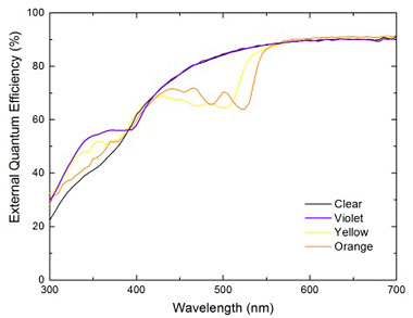
Figure: External quantum efficiency (EQE) curves for multi-crystalline silicon mini-modules exhibiting the enhancement of the short-wavelength response in the region 300-400 nm.
The use of luminescent materials with visible wavelength emission results in colouration of PV modules. This property is of particular interest for applications where aesthetics are important, such as building-integrated PV (BIPV).
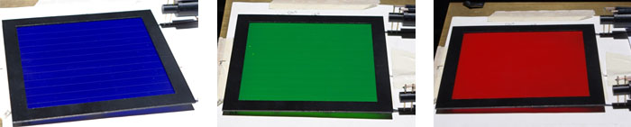
Figure: Three differently coloured CdTe mini-modules using LDS add-on layers.
Contact: Ian Howard
Down-Conversion of High-Energy Photons for Ultra-High Efficiency PV Modules
Down-Conversion (DC) otherwise known as quantum-cutting of a high energy photon to two lower energy photons can lead to significant gain in PV module efficiency. Our research focuses on using suitable lanthanide ion pairs that can be integrated in the PV module architecture.

Figure: The in-principle potential of the DC technology to result in external quantum efficiency (EQE) values in excess of 100% is shown for a luminescent material embedded in EVA encapsulation layer, which absorbs in the 300-500 nm region and emits with 200% PLQY.
Contact: Ian Howard, Andrey Turshatov,
Up-Conversion of Below Band-Gap Energy Photons for PV Devices
PV modules are transparent to photons with lower energy than the semiconductor’s bandgap. At IMT we develop materials that can perform up-conversion (UC) with high efficiency and the methodology to integrate UC layers to PV modules.
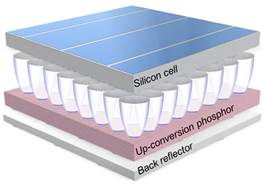
Figure: Schematic depicting an UC layer placed at the back of a silicon solar cell and concentrating lenses for increasing the local intensity of NIR photons incident to the UC layer.
Contact: Ian Howard, Andrey Turshatov
Luminescent Solar Concentrators
The luminescent solar concentrator (LSC) is a low concentration technology that has the potential to lower the cost of solar electricity by using inexpensive materials. The LSC is a particularly promising technology for the urban environment, as it offers a great degree of flexibility in shape, colour and system design. At IMT we investigate ways to increase the LSC efficiency and upscale the technology.
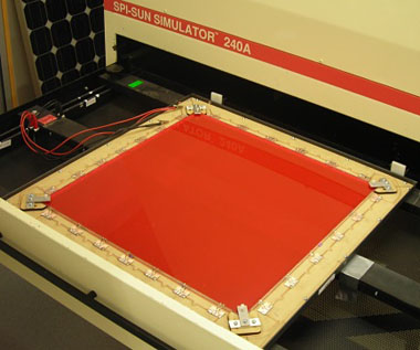
Figure: A large-area (60 cm ͯ 60 cm) LSC in a flash solar simulator for electrical characterization.
Contact: Ian Howard