

Dry Etching Cluster
Different dry etching technologies (RIE/ICP, RIBE) are used for micro and nano machining. First, the substrate is generally coated with a photoresist. The layout of the structure is then transferred into the resist layer by electron beam lithography. After developing the resist, the pattern of the resist mask is transferred into the substrate using dry etching. By parameter optimization it is possible to achieve anisotropic etch profiles, high aspect ratios and low mask undercut as well as to avoid stiction problems due to capillary forces. The gases used in our Dry Etching Cluster are among others SF6, CHF3, Cl2, BCl3 and HBr, allowing the structuring of a large variety of materials. Deep Silicon micro- and nanostructures are especially fabricated by Deep Cryo Etching. For very shallow silicon designs in the nm range HBr is the preferred gas. Finally, for metal layer systems different Cl- und F-based RIE processes are available. In particular, magnetic layers are patterned by Ion Beam Etching in the RIBE chamber.
The Dry Etching Cluster belongs to the KNMFi equipment. External users can apply for machine time by means of a proposal system at www.knmf.kit.edu.
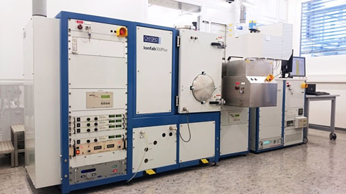 |
Overview of the RIE/RIBE Cluster (Oxford Plasmalab RIE100-ICP380, Oxford Ionfab 3000Plus) |
SEM
Characterization of structures and devices in the nanometre regime is a big challenge. Beforehand, electron-optical control of the structures in a scanning electron microscope (SEM) is essential. Hence, also the recording of the physical properties has to be done inside the SEM. For this purpose, nano manipulators are in use allowing to measure smallest electrical currents as well as the performance of electrical resistance. In parallel, it is possible to heat the nanostructures directly by applying an electrical current and to determine their actuation force.
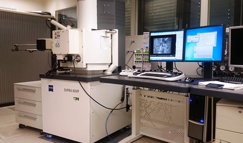 |
Overview of the SEM (Zeiss Supra 60VP) |
Contact:
Muslija, Alban Engineer