

Lithography
Historically, lithography is a method to print text or artwork onto e.g. paper by using a structured rigid plate. Several methods - which do not include engraving – exist to bring the structures onto the plate. Offset lithography is a still common form of printing technology.
Lithography in our context here means structuring materials on a fine scale below 10 µm (microlithography) or below 100 nm (nanolithography) using complex and mostly expensive equipment, particular chemicals and materials, electrons or light of different wave lengths and human expertise. The Institute of Microstructure Technology has been gaining expertise over many years in structuring diverse polymeric materials and selected metals down to the nanometer range.
Below you will find a survey of IMT’s capabilities in micro and nanolithography.
Electron Beam Lithography
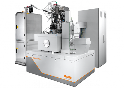
In 2015 an electron beam writer EBPG5200Z from Raith GmbH has been installed at IMT. The EBPG5200Z is a high performance nanolithography system with full 200 mm writing capability. Key features of the device are:
- High current density thermal field emission gun for operation up to 100 kV
- 200 mm platform for up to 8 inch wafer and 7 inch masks
- Minimum feature size of less than 8 nm
- Rapid exposure with 100 MHz pattern generator
- Continuously variable large field size operation to 1 mm
- GUI for ease of use operation
- Z-Stage to write substrates with different height levels
The electron beam writer is one of the KNMFi devices. External users get service via a proposal system at www.knmf.kit.edu.
Two-Photon Lithography
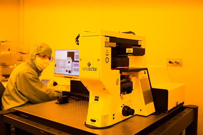
3D Direct Laser Writing is a tool to fabricate 3D freeform structures down sub µm. It is based on Two-Photon Lithography but beyond that 2D and 2.5D structures with nano dimensions are also possible. This system uses a nonlinear two-photon absorption process to modify, e.g. polymerize, a photosensitive medium at a specific point in the resist. By scanning the photoresist with a stage over this point a 3D-structure with dimensions in the submicron scale or greater can be written.
- Resolution:
3D: 200 nm lateral, 750 nm normal
2D: 180 nm - Feature structure size: max. 600 x 600 x 3700 µm³ depending on filling factor
- Writing modes: piezo (100x DIP), galvoscan (63x GT, 25x GT)
- Corresponding writing fields: 300 x 300 x 300 µm³; 140 x 140 µm²; 280 x 280 µm²
- Writing times: piezo slow, galvoscan fast
- Larger areas have to be stitched
- Accessible writing area: 100 x 100 mm² where structures could be placed
3D Direct Laser Writing is a technology which offers machine time to external users by the KNMFi.
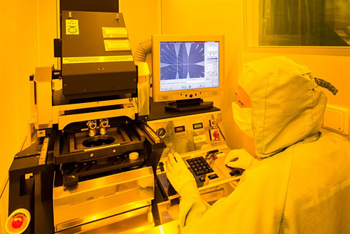
X-Ray Lithography
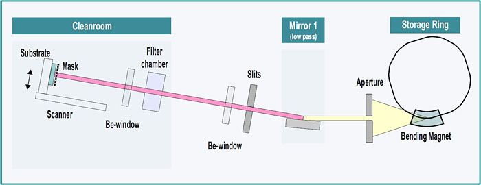
X-ray lithography is the first step of the well-known LIGA process which has been developed in the late eighties at KIT. XRL uses synchrotron radiation to pattern thick PMMA layers (thickness: several microns up to several millimetres) in order to achieve high aspect ratio microstructures (aspect ratio up to 50). The structures are characterised by very steep sidewalls (slope angle better than 1 mrad) and sidewall roughness in the range of 20 to 30 nm. For optical applications usually microoptical benches with cylinder lenses, prisms and fixing structures for other optical components are fabricated. Other examples are RF MEMS applications like antennas or lumped RF circuits and micromechanical devices. The structures are either used as prototypes, as lost form for metal replication or as moulds to fabricate mould inserts.
Features
- Aspect ratios up to 50 (>100 for special applications, under development)
- Structural height up to several millimetres
- Structural details less than 1 μm
- Slope angle better than 1 mrad
The XRL exposure stations are located at the Test Facility KARA and belong to the KNMFi equipment. External users can apply for service via a proposal system at www.knmf.kit.edu.
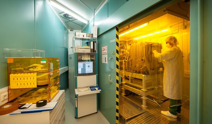
Direct Laser Writing
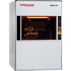
With Direct Laser Writing 2D-patterns in the µm-range are written in a photo resist layer on a substrate with a focused laser beam. No mask is needed as in conventional photo lithography.
The writehead allows feature sizes down to 2.5 µm with a substrate size up to 6”. The machine complements electron beam lithography and is a less expensive and faster alternative for structures without nano sized features. Typically this method is applied to generate first prototypes and allows a faster iteration.
Due to the used wavelength of 355 nm it is possible to pattern thicker resist layers (e.g. SU-8 type resists). The focusing of the laser beam leads in this case to sloped sidewalls (< 5°).
In case of reflective substrates a bottom antireflection coating (BARC) has to be applied, which may be considered in the whole process layout.
- No mask needed
- The wavelength of the laser (355 nm) allows to expose SU-8-resist up to 300µm thickness and AZ-resists up to 7µm thickness.
- Writing speed is 35 mm²/min. A 4“ wafer will be written in about 3 hours.
Direct Laser Writing is a technology which offers machine time to external users by the KNMFi.
UV Lithography
The EVG 620 Mask Aligner is available for standard UV-Lithography and Deep UV exposures with 250 nm wavelength. There is also the possibility of adjusted back side exposures for MEMS applications. The UV-Lithography team has many years of experience and there is a great variety of processes available with both positive and negative resists:
- AZ resists, negative and positive
- SU8, negative, very sensitive resist
- PMMA for Deep UV as positive resist