

LIGA Process


|
Using the LIGA process, microstructures can be manufactured from different plastic materials and metals. LIGA is a German acronym that stands for Lithographie, Galvanik und Abformung, i.e. X-ray Lithography, Electroplating, and Molding. The LIGA process was invented in the eighties at our institute and is being refined constantly to be able to meet today’s requirements regarding the materials, the properties, and quality of microstructures that are manufactured based on it. Large quantities of microstructures can be produced providing mold inserts for hot embossing or injection molding.
The LIGA process or structures manufactured using it are characterized by the following properties:
LIGA includes the following main steps:
Steps of the LIGA Process
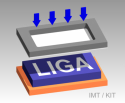
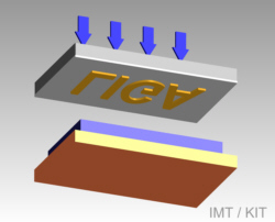
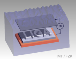
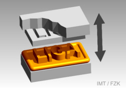
1. Fabrication of an Intermediate MaskThe intended microstructure is designed on the computer using a CAD system. The drawing is copied point by point by an electron beam writer into a plastic layer (the “resist layer”) that is deposited on a substrate (Fig. 1). As the drawing is copied, the electron beam moves over the substrate within close limits of 1.2 mm while the substrate, over greater distances, traverses under the electron beam. A silicon wafer with carbon layer sputtered over a 2 µm titanium layer mostly serves as substrate. At a later stage of the process, the sputtered titanium layer will serve as mask membrane carrying the absorber structures. The silicon wafer prepared that way is spin-coated with a layer of still liquid plastic (e.g. PMMA) of a thickness of approximately 3 µm and is hardened at elevated temperatures. Bombardment with high-energy electrons during the electron beam lithography process causes the long-chained molecules of the resist layer to be converted into short-chained ones, which can be dissolved selectively against the non-irradiated areas in the course of wet-chemical development. Subsequently, approximately 2 µm gold is deposited by electroplating on the titanium substrate where that is not covered any more with plastic (Fig. 2). While the gold will be serving as absorber material at a later stage since it strongly absorbs X-ray light, the titanium substrate has a high X-ray transparency due to its low atomic number. The non-irradiated resist is now removed completely by means of dry-etching, and a stable rectangular Invar alloy frame is glued onto the titanium surface. The titanium layer around the frame is scored or scratched mechanically and is carefully removed from the silicon wafer. This process is enabled by the carbon layer applied first having a comparatively poor adhesion on the silicon surface and allowing to lift off the titanium membrane with the frame and the gold absorber deposited on it. The X-ray contrast of the intermediate mask (2 µm Au on 3 µm Ti) suffices for deep X-ray lithography structuring of plastic layers with thicknesses of up to 70 µm. Since mostly rather higher structures are of interest, a working mask with higher X-ray contrast is often produced from the intermediate mask. 2. Fabrication of a Working MaskFabrication of a working mask is quite similar to fabrication of the intermediate mask. Working masks, however, are not structured by means of electron beam lithography but are produced by copying the gold structures of an intermediate mask in a PMMA resist layer of approximately 60 µm by means of deep X-ray lithography (Fig. 3), which causes formation of short-chained molecules, too. After development, 25 µm gold absorbers are deposited by electroplating in the areas exposed, and the non-irradiated resist is removed (Fig. 4). Due to the higher X-ray contrast, a working mask suffices for structuring resist layers with thicknesses of some millimeters by means of deep X-ray lithography. 3. Fabrication of High MicrostructuresOnce the working mask has been manufactured, it can be used as a tool for deep X-ray lithography structuring of PMMA resist layers with thicknesses of up to 3 mm (Figures 5 and 6). PMMA layers of such thicknesses, as a rule, are glued to the substrate as foils. Fabrication of the direct-lithography PMMA microstructures is concluded as described above by wet-chemical development of the irradiated areas of the PMMA layer (Fig. 7). 4. ElectroformingUsing the LIGA process, metallic microstructures are produced by electroforming. A direct-lithography microstructure manufactured as described above is immersed in an electrolytic bath, and a metal (mostly gold or nickel) is deposited in the irradiated areas (Fig. 8). As a prerequisite the substrate must be electric conductive which can be achieved by an appropriate pre-treatment. If one does not wish to use these metallic microstructures as they are, the electroplating process is continued until the metal coalesces over the PMMA layer to form one piece of metal from which a mold insert having some mm in thickness and with microstructured surface can be manufactured mechanically (Fig. 9). The material preferred in practice is nickel. 5. Mass Production by Means of Hot Embossing or Injection MoldingGiven appropriate conditions, microstructured mold inserts can be used several thousand times to transfer the attached microstructures into various plastic materials by means of hot embossing or injection molding and copy them that way (Fig. 10). These methods enable low-cost manufacturing of microcomponents. |