

Projects
We explore the mechanical, physical and chemical properties of nano- and micromechanical structures. Current research projects are
Biomimetic surfaces

Some animals and plants show fascinating surface effects caused by their specific microscopic surface structure. We analyse these phenomena with the atomic force microscope and frequently it is possible to mimic them using nano- and microreplication techniques (cooperation with Replication).
Many plants and insects possess multifunctional surfaces covered with dense nanohairs. Such nanofur is of high interest for various biomimetic applications like self-cleaning, self-healing, air retention, and oil-water separation. We introduced a highly scalable and competitive molding technique for biomimetic nanofur fabrication [1]. With this method, we pull nanofur out of flat polycarbonate sheet and thus, tune its wettability from hydrophilic to superhydrophobic. By mechanical structuring these samples we create various devices suitable for microfluidics. Moreover the nanofur can be used for the fabrication of self-healing surfaces inspired by pitcher plants and for air-retaining surfaces which mimic the water fern Salvinia. Finally, we utilize the nanofur for oil/water separation and the cleaning up of oil spills.
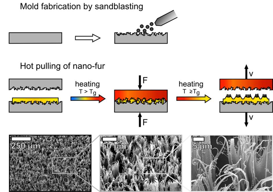
Figure 1: Schematic of the hot pulling process. A sandblasted steel plate is used to pull nanohairs out of a polymer sheet.
The main advantage of the introduced fabrication technique is that it can be used with several kinds of polymers. Nanofur can even be produced from so-called ”liquid wood”, a recyclable and biodegradable biopolymer based on lignin and wood fibers [2]. The as-prepared microhaired material absorbs crude oil out of the water and separates oil/water mixtures. Furthermore, its surface properties can be changed to hydrophilic and underwater superoleophobic by a short argon plasma treatment cycle, making the microhaired wood-based material capable of both ”oil-removing” and ”water-removing” oil/water separation methods.
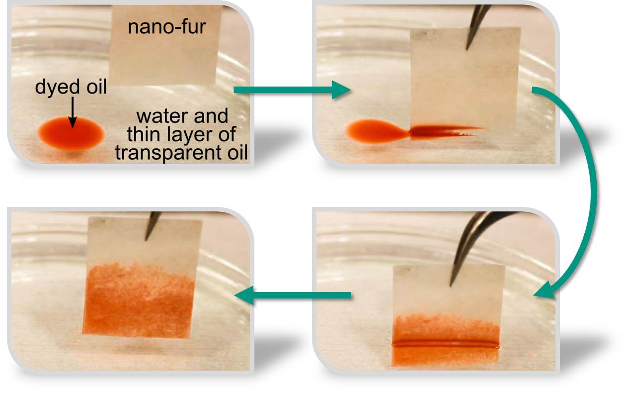
Figure 2: Demonstration of the cleaning of an oil spill with nanofur.
The nanofur has such strong water repellency that it does not get wet under water and is covered still covered by air when pressed under water [1]. Such air-retaining surfaces are known to reduce drag in fluids. Therefore, nanofur is also a solution for drag reduction in fluidics.
Publications
- Michael Röhrig, Matthias Mail, Marc Schneider, Henri Louvin, Andreas Hopf, Thomas Schimmel, Matthias Worgull, Hendrik Hölscher. Hot Pulling of Nanofur for Biomimetic Applications. Adv. Mat. Interfaces 1, 1300083 (2014)
- M. N. Kavalenka, A. Hopf, M. Schneider, M. Worgull and H. Hölscher, Wood-based microhaired superhydrophobic and underwater superoleophobic surfaces for oil-water separation, RCS Advances 3, 31079 (2014)
- Maryna N. Kavalenka, Felix Vüllers, Simone Lischker, Claudia Zeiger, Andreas Hopf, Michael Röhrig, Bastian E. Rapp, Matthias Worgull, and Hendrik Hölscher, Bioinspired Air-Retaining Nanofur for Drag Reduction, ACS APPLIED MATERIALS & INTERFACES 7, 10651 (2015)
This project is supported in part by the ZEISS-Foundation through a personal Ph.D. scholarship for Claudia Zeiger and by the Landesgraduiertenförderung through a personal Ph.D. scholarship for Felix Vüllers.
Contact
Dr. Maryna Kavalenka, M. Sc. Claudia Zeiger, Felix Vüllers

Figure1 : Comparison of a Morpho Rhetenor with its artificial copy [3].
Nature offers a great source of inspiration for developing next generation optical applications. Many natural photonic structures are multifunctional and can be used in many applications. The wing of the Morpho butterfly is a great example of multi-functionality. An evolutionary optimized nano-structure in the scales of this butterfly also gives a strong blue coloration and makes the wing hydrophobic [1,2]. Because of these multiple features of the butterfly scales, biomimetic/replication of the micro/nanostructure especially on a large scale is extremely interesting for industrial applications [2,3]. Moreover, exploring unknown features of different butterfly’s scales using optical modeling techniques is important to tune and explore the optical properties of such structures for the desired functionality.
Publications
- R H. Siddique, S. Diewald, J. Leuthold and H. Hölscher, Theoretical and experimental analysis of the structural pattern responsible for the blue irradiance of Morpho butterflies, Optics Express 21, 14351 (2013).
- Radwanul Hasan Siddique, Abrar Faisal, Ruben Hünig, Carolin Bartels, Irene Wacker, Uli Lemmer, Hendrik Hölscher, Utilizing laser interference lithography to fabricate hierarchical optical active nanostructures inspired by the blue Morpho butterfly, in The Nature of Light: Light in Nature V, Rongguang Liang; Joseph A. Shaw, Editors, Proceedings of SPIE Vol. 9187 (SPIE, Bellingham, WA 2014), 91870E.
- Norbert Schneider, Claudia Zeiger, Alexander Kolew, Marc Schneider, Juerg Leuthold, Hendrik Hölscher, and Matthias Worgull, Nanothermoforming of hierarchical optical components utilizing shape memory polymers as active molds, Optics Materials Express 4, 1895 (2014)
- Radwanul Hasan Siddique, Ruben Hünig, Abrar Faisal, Uli Lemmer, and Hendrik Hölscher, Fabrication of hierarchical photonic nanostructures inspired by Morpho butterflies utilizing laser interference lithography", OPTICAL MATERIALS EXPRESS 5, 996 (2015)
- Radwanul H. Siddique, Guillaume Gomard, and Hendrik Hölscher, The role of random nanostructures for the omnidirectional anti-reflection properties of the Glasswing butterfly, NATURE COMMUNICATIONS (2015)
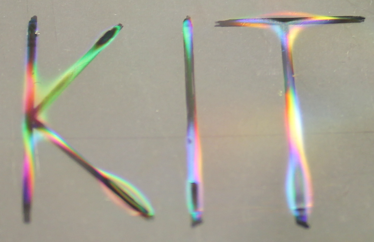
Figure 1: Demonstration of the shape memory effect. A grating programmed into a shape memory polymer is locally recovered by heating and the recovered areas (“KIT”) reflect blue and green light.
Nearly all consumer good of our everyday life are manufactured from polymers colored by dyes. This approach allows endless variety of colors of houseware, clothing, cars, and interior decorations offered by industry. Today, each item is produced in one color which cannot be changed. It is widely assumed that a large amount of items will be produced by 3D printing in the future in order to spare molds and shipping of rarely used parts.
Our approach goes ahead this printing-on-demand approach. We want to produce polymer surfaces which can change their color. In this way consumer goods can be stockpiled and their color can be chosen shortly before delivery. The ultimate aim is a consumer product as a car in which complete interior can be colored on demand shortly before delivery to the costumer.
Changing colors are infrequently observed for camouflage in nature. The most prominent examples are chameleons and octopuses that change the color of their skin which the help of pigments in their cells. This approach is not practical for everyday goods. Therefore, our approach is to combine the effects of smart polymers, nanoparticles, and structural colors.
Shape memory polymers (SMPs) can transform their shape from a temporary shape back to a programmed permanent shape by a trigger like heat (see figure at the top). In this way, for example, it is possible to change the period of gratings which in turn changes the emission wavelength of a DFB laser [1].
- Senta Schauer, Xin Liu, Matthias Worgull, Uli Lemmer, and Hendrik Hölscher, Shape-memory polymers as flexible resonator substrates for continuously tunable organic DFB lasers, OPTICAL MATERIALS EXPRESS 5, 576 (2015)
Contact
Dipl.-Ing. Senta Schauer
Scanning Probe Technologies
The analysis and development of new techniques for the microscopy and spectroscopy of surfaces on the nano-scale allows new insights into the nanoworld.
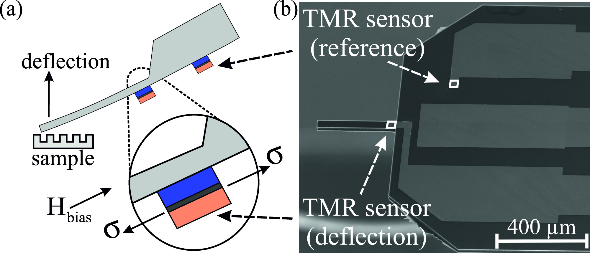
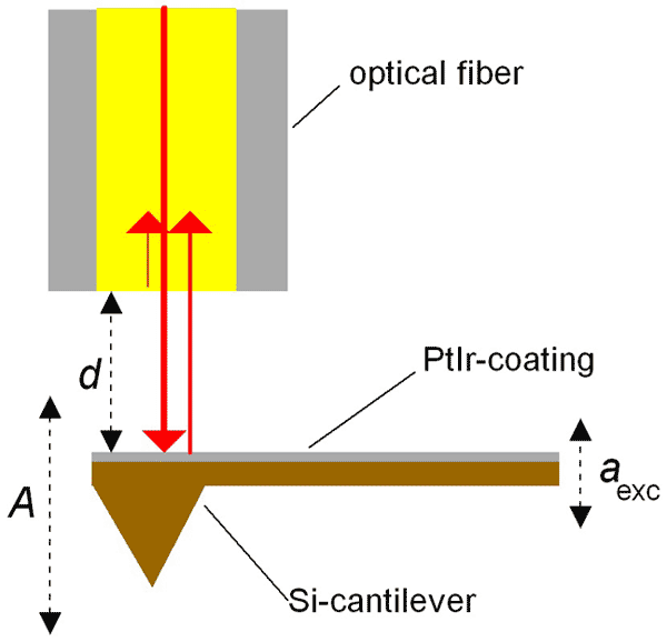
Figure 1: a) Schematic of a cantilever with TMR sensor and b) the realization [1].
We use magnetostrictive tunneling structures as highly sensitive strain sensors to enable new applications of atomic force microscopy with self-sensing cantilevers. With this aim, the miniaturization of the strain-sensitive tunneling structures will be pushed forward to submicron scales and supported by micromagnetic simulations. The comparison between simulation and experiment contributes to the understanding of the magnetization reversal in mechanically stressed magnetostrictive structures, finally leading to an increased control of their magnetization configurations. This in turn has a direct impact on the long-term stability of the sensors.
Through the planned development of the layer system of tunneling structures, we aim on the one hand on the increase of sensitivity and signal to noise ratio. On the other hand, an internal magnetic bias field will be implemented into the layer system, in order to eliminate the need for an external bias field to measure at an optimal operating point. For this purpose we apply the concept of a sensor electrode coupled to an antiferromagnetic layer sensor, which has been very successful in solving a similar problem with magnetoelectric magnetic field sensors.
With these new self-sensing cantilevers we carry out atomic force microscopy experiments under ambient conditions, in vacuum, and in liquids on different sample systems. Our focus is on applications where conventional optical detection system of conventional AFMs can be detrimental. Furthermore, we will build and analyze cantilevers with multiple strain sensors for friction force and multi-frequency measurements.
- A. Tavassolizadeh, T. Meier, K. Rott, G. Reiss, E. Quandt, H. Hölscher, and D. Meyners. Self-sensing atomic force microscopy cantilevers based on tunnel magnetoresistance sensors. APPLIED PHYSICS LETTERS 102, 153104 (2013)
- Tobias Meier Alexander Förste, Ali Tavassolizadeh, Karsten Rott, Dirk Meyners, Roland Gröger, Günter Reiss, Eckhard Quandt, Thomas Schimmel, and Hendrik Hölscher, A scanning probe microscope for magnetoresistive cantilevers utilizing a nested scanner design for large-area scans, BEILSTEIN JOURNAL OF NANOTECHNOLOGY 6, 451–461 (2015)
This project is a cooperation together with Dirk Meyners (CAU Kiel) and Günter Reiss (University of Bielefeld). It is supported by the DFG (HO 2237/4–1 and HO 2237/4–2)
Contact
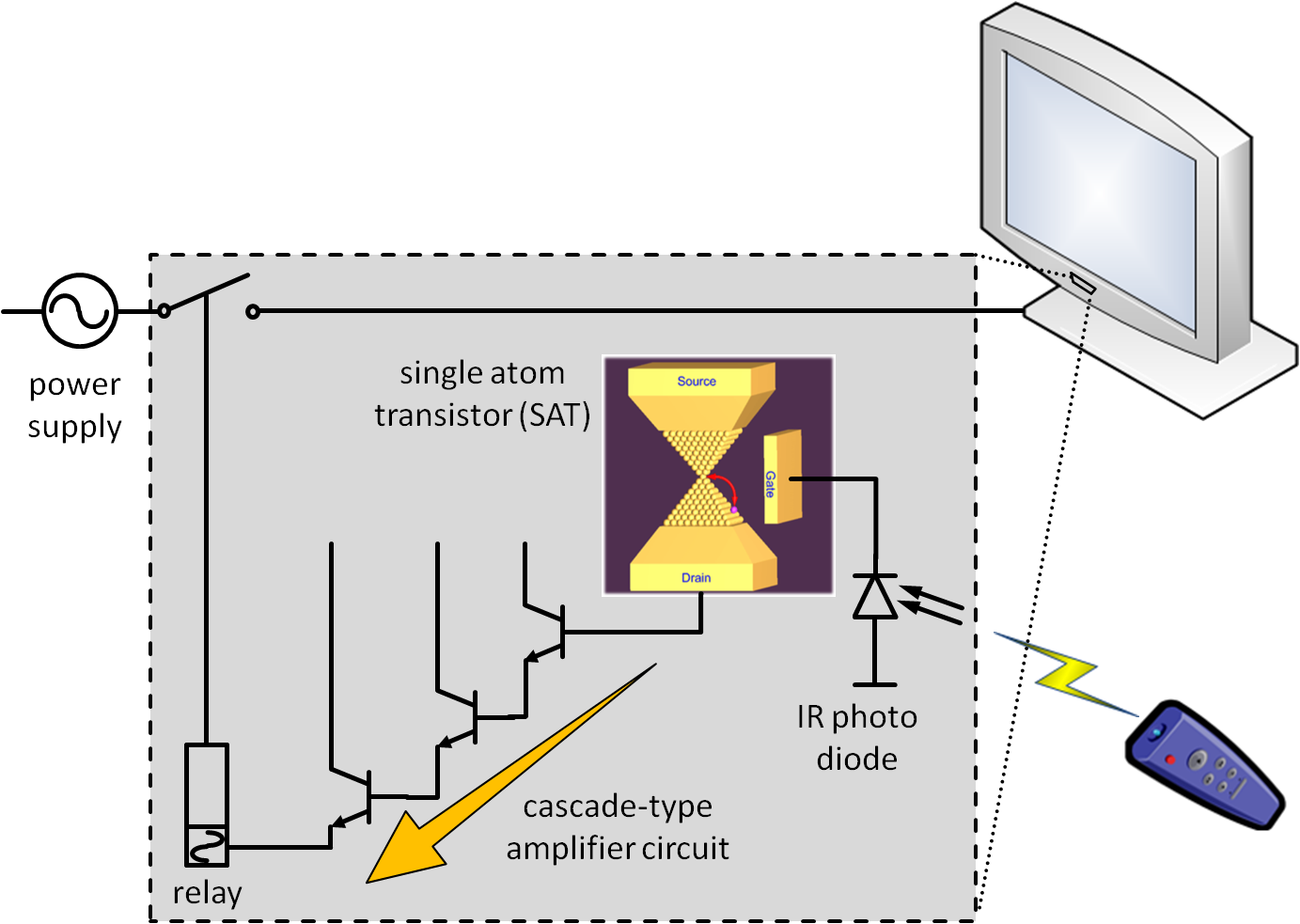
Figure: Schematic of the envisioned single-atomic standby switch. The extremely sensitive single atomic transistor (SAT) is switched on through the gate voltage supplied by the infrared (IR) photodiode. This trigger starts the cascade-type amplifier circuit which finally switches the power supply of consumer electronics like TV sets or hi-fi units. In this project we optimize the SAT and integrate it into a micro-structured planar device which is finally connected to the cascade-type amplifier circuit.
Standby switches are an omnipresent part of nearly all electronic devices in our homes and cause the loss of about 6.5% of the annual electricity consumption of an average household. Due to the enforced reduction of these losses industry is currently searching for solutions. The most important issue, however, is the energy loss caused by standby devices which are neither in power down nor in active operation because they are still addressable for a remote control signal. Typical examples are TV sets, DVD players or i-fi units which are present in every household. Consequently, these three remote controlled device categories are responsible for more than 50% of the wasted standby power.
Therefore, it is the aim of the project to realize a standby switch based on a single atomic transistor with nearly zero power consumption. While the project targets the power loss in households due to standby operation of electronic devices it envisions a broader project goal: the first exemplarily demonstration of the potential enabled by a new generation of single atomic devices. In a first phase we optimize and realize a single atomic transistor that has previously been demonstrated at KIT in the group of Prof. Schimmel. We will then integrate it within a nano- and microstructured device, and develop a cascade type electric circuit in order to enable the reliable “on” and “off” switching of an electric device.
This project is a cooperation together with Thomas Schimmel (KIT) and Jürg Leuthold (ETH Zürich). It is supported by the VW-Foundation (2012–2016).
Contact
Dr. Maryna Kavelenka, PD Dr. Hendrik Hölscher
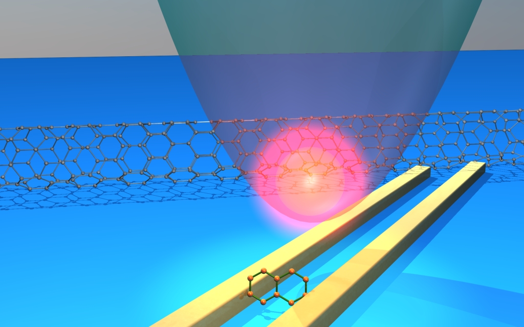
Figure: An artists view of „Cold Atom Scanning Probe Microscopy & Spectroscopy“. An ultra-cold atom cloud in a magnetic trap scans a surface in all three dimensions. The dynamic of the atom cloud in the parabolic potential is used to determine the sample topography as well as electromagnetic fields and dispersion forces.
Atomic force microscopy (AFM) is the work-horse among all scanning probe microscopy (SPM) methods since it allows the imaging of surfaces down to the atomic-scale in liquids, vacuum, and ambient conditions. The sample topography as well as elastic, magnetic, electrical, thermal, and chemical properties can be recorded with high spatial resolution. As in all scanning probe techniques, however, it is a weakness that the exact tip shape and the chemical identity of its apex atoms are commonly unknown. Therefore, it is extremely difficult to directly compare experimentally recorded tip-sample interactions with theoretical models.
A way out of this dilemma is the subject of the project: in cold atom scanning probe microscopy (CA-SPM) the tip is replaced by a gas of ultra-cold Rubidium atoms that is confined inside an electromagnetic trap representing the cantilever. Such a cold-atom SPM can be operated in a dynamic mode by making the gas oscillate within the trapping potential and measuring how the oscillation frequency changes as the trap is scanned over the surface. Since the interaction potential between the cloud and the sample slightly modifies the potential of the trap, the oscillation frequency of the cloud is changed and the interaction potential can be calculated from the frequency shift. Interestingly, the theory behind the dynamic mode of CA-SPM and the theory of the dynamic force spectroscopy that has been developed for AFMs is essentially the same [1,2]. Therefore, it is very promising to combine these techniques and for measuring the interactions between the atoms of the gaseous probe tip and a sample surface.
This project combines the expertise of three groups located in Tübingen (J. Fortágh), Karlsruhe (H. Hölscher) and Stuttgart (K. Balsubramanian) in the fields of cold atoms, scanning probe microscopy, and functional nanostructures, respectively. It is supported by the BW-Foundation (2012–2014).
- H. Hölscher: Cold atoms feel the force. Nature Nanotechnology 7, 484 (2012)
- Andreas Günther, Hendrik Hölscher, József Fortágh, Cold-Atom Scanning Probe Microscopy. In: Fundamentals of Picoscience (ed. by Klaus Sattler), Taylor & Francis (2013)