Nanophotonic Light Management
Nanophotonic materials offer novel routes to tailor the light propagation and light coupling in optoelectronic devices. In close collaboration with the Light Technology Institute (LTI) at KIT, IMT researchers engineer and prototype nanophotonic light management concepts for photovoltaics, LEDs and solar energy. Our work involves the fabrication, characterization and optical simulation of nanophotonic light management concepts.

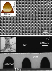
Light-trapping structures allow incident light to be guided in the absorber layer of a solar cell. This way, the absorptance of light in the solar cell can be enhanced beyond the absorption of a single light pass through the device. Nanophotonic light trapping structures make use of nanostructured matter and photonic crystals and, thereby, offer particular functionalities to tailor the propagation of light and are compatible with thin absorber layers.
For more information see Ulrich Paetzold and Bryce Richards.

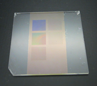
Nanophotonic electrodes offer exciting potential to enhance light in-coupling at the front side of thin-film solar cell. The electrodes exploit the nanophotonic functionalities of photonic crystals, dielectric gratings, and guided modes. The fabrication and replication of nanostructures makes use of the unique facilities at IMT.
For more information see Ulrich Paetzold.

Nanophotonic structures are exploited in LEDs to improve the outcoupling of the generated light, which is otherwise trapped within the devices as guided modes, and for beam shaping purposes. To this end, periodical nanostructures as well as stochastic (scattering) ensembles are developed both numerically and experimentally at the IMT with of view of realizing these photonic elements over large areas, for example using printing techniques.
For more information see Uli Lemmer.

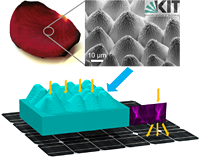
Many plant and animal species control the flow of light thanks to a great variety of photonic structures, ranging from periodical to highly disordered ones. We aim at analyzing such structures by the means of spectroscopy measurements and optical simulations to retrieve essential design rules that enable us to produce bio-inspired coatings applied to optoelectronic devices. Since biostructures usually serve for different purposes, this biomimetic route allows us to achieve multifunctional coatings.
For more information see Hendrik Hölscher and Ulrich Paetzold.

