

3D Photonic Integration (3PI)
Dr. Klaus Bade [Contact]
Welcome
The activities of the group aims to further develop and optimize the process technique to pattern structures by laser lithography and to produce 3D structures by 2-photon laser lithography (3D-laser writing). Although these technologies are part of our technology offer of the open access research infrastructure KNMFi we intend to continuously upgrade the technologies according to application needs and to depict the value of the technologies in various applications which are part of strategic activities of the program Science and Technology of Nanosystems.
Our research contributes to the research program 3: "Materials Systems Engineering" (MSE), Topic 2: "Optics and Photonics: Materials, Devices and Systems", in the research field „Information“ as defined by the Helmholtz Association. Link to MSE website.
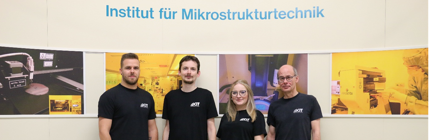 Members of the laser lithography group in front of pictures oft their working environment
Our activities in laser lithography rely on the use of the Heidelberg Instruments DLW66 fs. This tool gives us the opportunity to pattern structures on wafers (up to 6 inch) with lateral dimension down to 3 µm and heights up to 300 µm depending on the used resists. This results in an aspect ratio of 5 to maximum 10. One focus of our activities is to combine this technology with other microfabrication technologies to achieve multi scale structures with structural functionality. Further process development of thick resist layers to achieve corresponding structural heights is going on. This activity includes proper application of antireflection coatings and adhesion promotors, as well as proper resist processing.
3D laser writing by 2-photon lithography takes advantage of the fact that the change of resist during exposure is confined in a very small ellipsoidal volume (short 200 nm, long 600 nm). Moving this volume (voxel) allows the formation of 3D freeform structures. For running the process we are using a Photonic Professional GT from Nanoscribe. Several writing configurations with different objectives and resists can be applied as well as fast scanning in the x,y-plane by a galvoscan unit. With equipment from 3i- Intelligent Imaging Innovation we are exploring the application of structured light by usage of a Spatial Light Modulator (SLM) for new writing approaches. We are looking for improving the writing procedures by development of new writing strategies especially for larger areas or volumes. Stitching volume elements and shell-writing with following flood exposure are examples. Additional new resist formulations are investigated in cooperation.
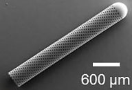
Lithography based Ceramic Manufacturing (LCM) supplements our activities with respect toward microstructured ceramic components. We use CeraFab S25 from Lithoz GmbH to manufacture parts out of alumina, aluminum nitride and silicon nitride with dimensions from the upper µm-range to 30 mm x 50 mm x 240 µm with a resolution of about 25 µm.
|
|
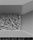
Nanopatterned structures in a µm-sized fluid channel realized by combining 2D and 3D laser writing. |
|
|
|
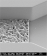
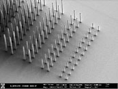
Pillar array with increasing height and sub-µm diameter printed by 2-photon lithography. |
|
|
|
Examples of printed ceramic parts (Al2O3) by LCM. |
Read more…
 |
 |
 |
||
| Nanopatterned structures in a fluid channel realized by combining 2D and 3D laser writing. |
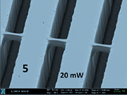
Bridge structure fabricated by 2D laser lithography with well optimized laser power to connect resist lines patterned in UV lithography. |
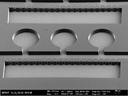
Polymeric microfludic chip with barrier structures (cylinders) and reservoirs made by direct laser writing. The resist thickness is 50 µm. |
 |
 |
 |
||
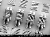
| Scaffold structures for evaluation of cell attachment and growth made by 3D direct laser writing. | Large microfluidic component. | Pillar array with increasing height and sub-µm diameter. |
Teaching, Education, Jobs
As a member of KNMFi we are offering technology specific training courses.
Klaus Bade gives lectures at the Department of Mechanical Engineering under the topic:
Fertigungsprozesse der Mikrosystemtechnik ( / )
Open Ph.D. positons will be advertised on KIT’s website for job offers.
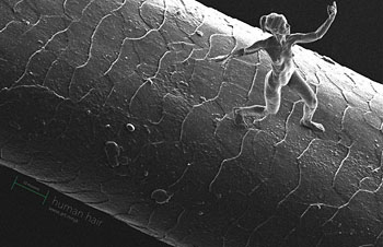
In collaboration with the British artist Jonty Hurwitz an the KNMF (KNMF) a sculpture of a woman with a height of only about 100 µm was made in IMT’ s laboratories. For pictures and a CNN video from the making of please visit: www.jontyhurwitz.com/nano/