

Welcome
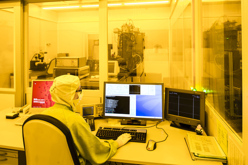
to the Advanced Nanofabrication group, we focus on the fabrication of nano and micro structures by electron beam lithography as well as preceding and following clean room processes. Ongoing projects aim at photonic devices, plasmonic devices and biophotonic sensors. Within KNMFi the Advanced Nanofabrication group offers electron beam lithography through the open access research infrastructure for academical or industrial partners.
Our research contributes to the research program 3: "Materials Systems Engineering" (MSE), Topic 2: "Optics and Photonics: Materials, Devices and Systems" (Subtopic 3: Designed Optical Devices & Systems), in the research field „Information“ as defined by the Helmholtz Association. Link to MSE website.
Electron Beam Lithogaphy
For electron beam lithography we use an EBPG5200Z from Raith GmbH. The EBPG5200Z is a high performance nanolithography system with full 200 mm writing capability. Key features of the device are:
- High current density thermal field emission gun for operation up to 100 kV
- 200 mm platform for up to 8 inch wafer and 7 inch masks
- Minimum feature size of less than 8 nm
- Rapid exposure with 100 MHz pattern generator
- Continuously variable large field size operation to 1 mm
- GUI for ease of use operation
- Z-Stage to write substrates with different height levels
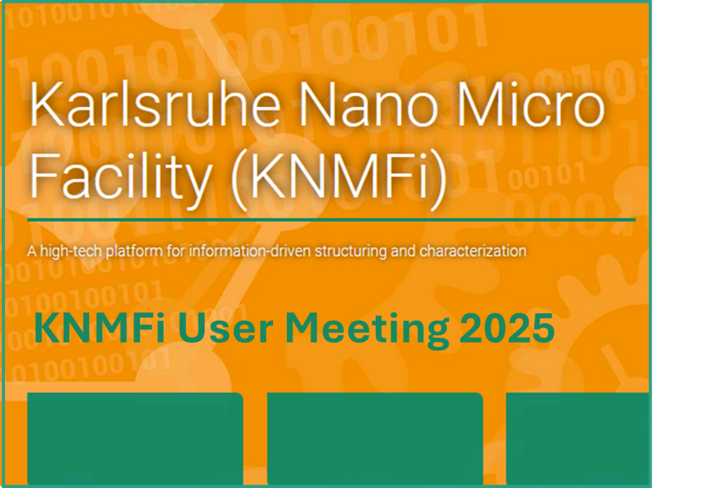
Karlsruhe Nano and Micro Facility (KNMFi)
KNMFi (Link) is a high-tech platform for information-driven structuring and characterizing a multitude of functional materials at the micro- and nanoscale. It offers access to a uniquely complete set of fabrication, characterization and information technologies. External users from academia and industry, either national or international, can apply for open and – if the results are published – free access. Annual deadlines for the submission of proposals are January 15 and June 15 (Link to proposal submission).
_rdax_1230x820s.jpg)
Day 1, Monday 03 November
Behind the Scenes Tech Tour (at KIT, Campus North)
including lab visits, presentations and discussions with KNMFi experts
17:00h: Electron Beam Lithography (EBL)
Day 2, Tuesday 04 November
KNMFi Proposal Spotlights
13:30 Precise Filling of Hollow Nanospheres with Magnetic Nanoparticles
Esther Rösch (Duale Hochschule Karlsruhe, Germany), Richard Thelen (KIT/IMT), Judith Hohmann (KIT/IMT)

Congratulations to Yuhao Wang (Center for Quantum Technology Research and Key Laboratory of Advanced Optoelectronic Quantum Architecture and Measurements, School of Physics, Beijing Institute of Technology). Our collaborative publication, ‘Miniaturized Single-Photon Level Computational Complex Field Imaging System via Meta-Optics’, was highlighted with a cover in Advanced Optical Materials.
More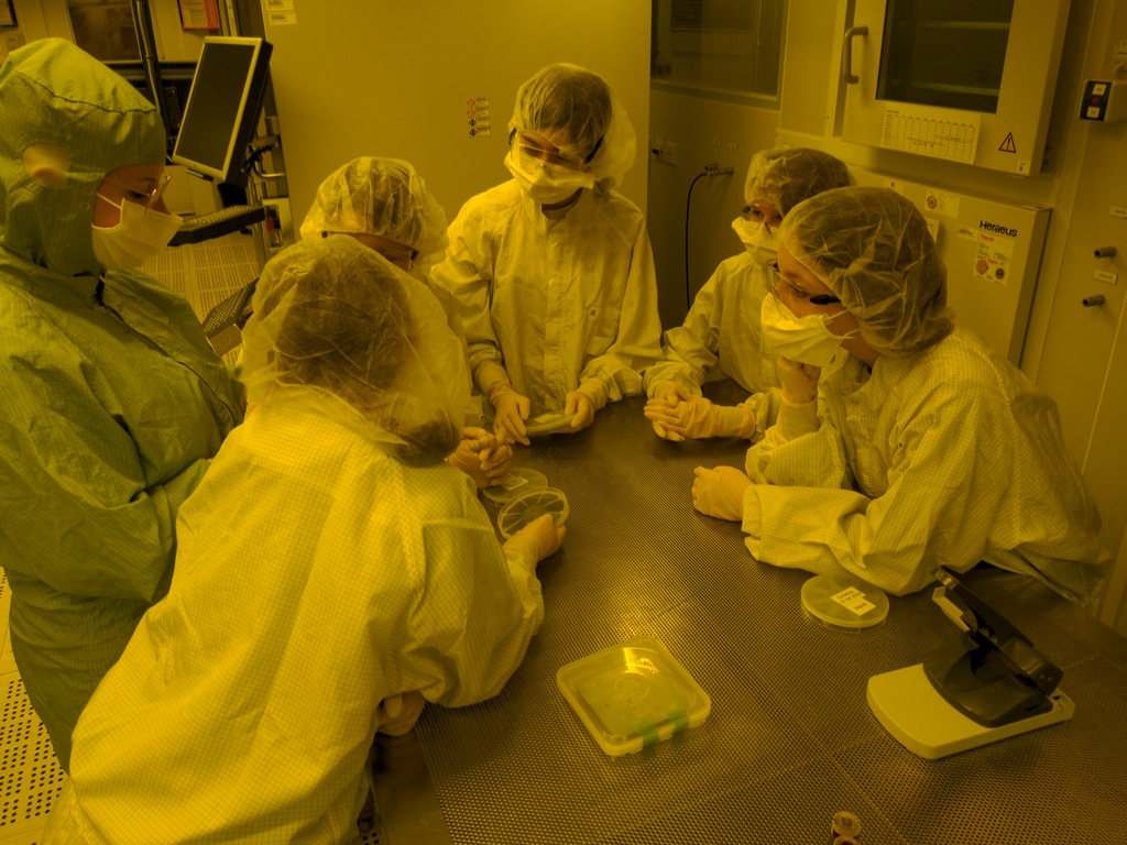
At the Karlsruhe Institute of Technology (KIT), schoolgirls were able to gain an insight into technical professions at the beginning of April as part of Girls' Day. One of the highlights was the workshop “A metal mouse in the clean room” at the Institute of Microstructure Technology (IMT), where five participants experienced lithography and electroplating in a practical setting. The students produced two-dimensional metal mice in the cleanroom and learned about the fascinating world of microstructures. In the final microscopy unit, they discovered secret details that were invisible to the human eye.
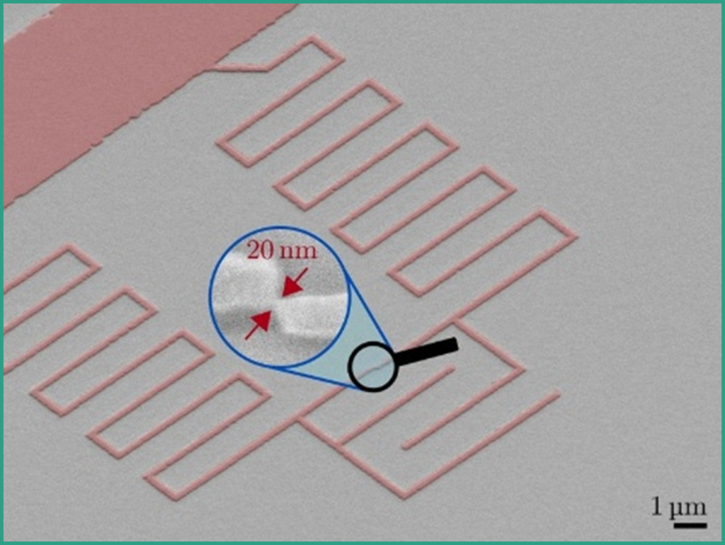
Quantum computers are considered to be the computers of the future. Quantum bits (qubits), the smallest computational unit of quantum computers, are the be-all and end-all. Because they have not only two states, but also states in between, qubits process more information in less time. However, maintaining such a state for a longer time is difficult and depends in particular on material properties. A KIT research team now generated qubits that are 100 times more sensitive to material defects – a crucial step toward eliminating them. Electron Beam Lithography (EBL, Link), a KNMFi technology, was the key technology to fabricate 20 nm small nanojunctions. The team published the results in the journal Nature Materials (DOI: 10.1038/s41563-022-01417-9).
Link to the press release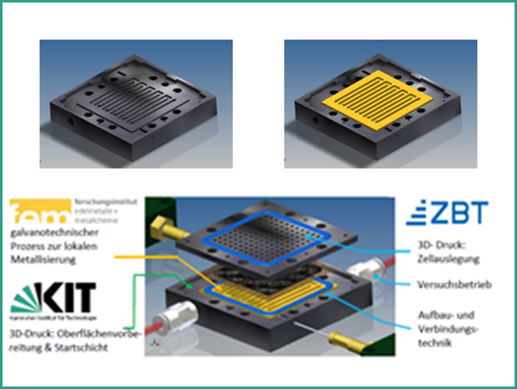
In the IGF project “Sensorzelle”, we are working with the Center for hydrogen and fuel cell (ZBT) and the Research Institute fem to develop a manufacturing process for flexibly designed test and sensor fuel cells based on 3D printing and electroplating technology.