

Nanoactuators
Micro- and Nanoactuators
Our activities aim at the development of mechanically active nanostructures showing sensing and actuation functions to pave the way towards a new generation of smart nanosystems. A key issue is the development of reliable processes for the fabrication of nanostructures of smart materials having critical dimensions below 100 nm. Novel in-situ measurement methods are required to characterize their physical properties on the nanometer scale. In these dimensions, scaling as well as coupling effects occur. Their understanding is a prerequisite for the design of nanodevices.
Shape memory alloys (SMAs) are highly suited for submicrometer applications due to their high work density and favourable scaling properties, but challenges such as temperature gradients and partial phase transformations limit their performance. To address these, we focus on temperature homogenization to improve actuation efficiency and explore bistable designs in nanoactuators to enable stable, large-force movements.
Out-of-Plane Microactuator
In-situ SEM experiments using nanomanipulators demonstrate the enhanced performance characteristics of the temperature-homogenized design of SMA microactuators. The figure illustrates typical experiments conducted on a double-beam microactuator made of TiNiHf/Si. Electrical resistance and deflection measurements confirm the shape memory effect through electro-thermal actuation via Joule heating.
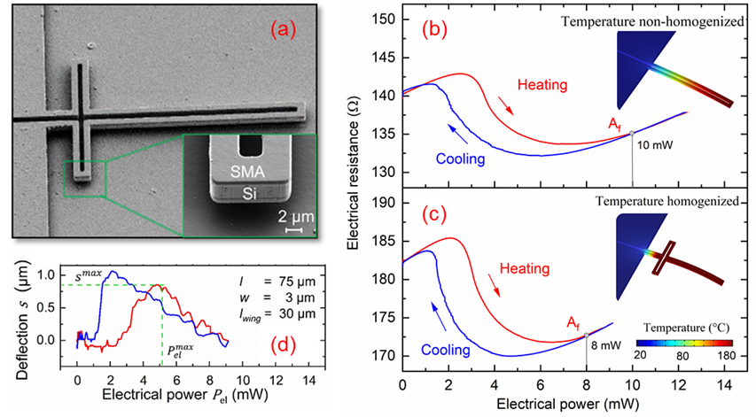
Figure 1: The in-situ SEM image of a freestanding TiNiHf/Si microactuator a) with temperature-homogenized wing design (b,c) electrical heating/cooling cycle and corresponding electrical resistance of a TiNiHf/Si microactuator: temperature non-homogenized and temperature homogenized design with wing-structure. Insets: FEM simulation of temperature profiles, d) deflection measurement of temperature-homogenized design with wing-structure. The wing structure design improves actuation stroke by 37% and reduces power consumption by 44% [1-4].
Bistable In-Plane Microactuator
Within the framework of the DFG Priority Program KOMMMA (more information at www.spp-kommma.de), we are developing small-scale, in-plane SMA microactuators capable of lateral movement between two stable states, leveraging the shape memory effect. The design employs two coupled prestrained SMA beams with nano-scale hinge dimensions, designed to exhibit buckling instability. Selective Joule heating activates the one-way shape memory effect in the SMA, generating a large shape recovery force that facilitates switching between the stable states.
Currently, we have successfully downscaled an in-plane bistable mechanism to the micro scale using silicon technology and investigated the bistability limits of a first demonstrator device. The force-displacement characteristics reveal the force barrier required for bistable switching, along with the negative stiffness behavior. Both the maximum reaction force and the corresponding critical displacement are in good agreement with our simulation results.
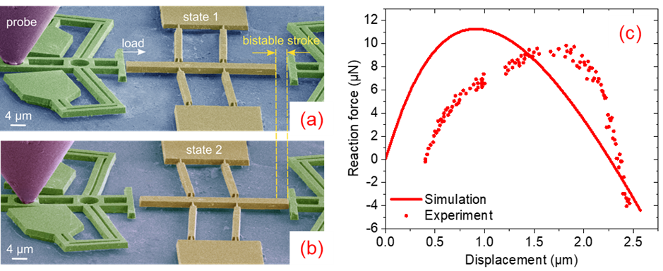
Figure 2: SEM images of a bistable silicon microdevice of footprint 80 x 40 µm2 and two silicon adaptor structures on either end of the microdevice for bidirectional actuation by the mechanical load of an in-situ nanomanipulator (see conical probe). (a) and (b) display the bistable positions (states 1 and 2), (c) experimental and simulated reaction force versus displacement of a bistable silicon microdevice with hinges of 300 nm width [4,5].
These actuators may be combined with Si waveguide structures to develop novel active photonic devices such as nanooptical switches or tunable nanooptical devices. For this purpose, a process flow has been developed to simultaneously fabricate double-beam SMA-Si-bimorph cantilevers, Si waveguide structures and grating couplers on a common SOI wafer, with 340 nm device layer thickness and 2 μm SiO2 layer thickness. Fabrication comprises two-step electron beam lithography (EBL) and pattern transfer to Si by reactive ion etching (RIE).
Funding/ Projects
DFG Project “Cooperative SMA Actuator Systems for Nanomechanics and Nanophotonics”
This project is part of the DFG Priority Program “KOMMMA”, which bundles the research of 18 Principal Investigators over 6 years. Objectives of this interdisciplinary program are to show up new methods and concepts to understand the complex coupling and synergy effects in coupled microactuator systems as well as to fabricate platforms for cooperative and/or multistage microactuator systems.
LINK to KOMMMA DFG Priority Programme
![]()
Publication List
- Curtis, S. M., Sielenkämper, M., Arivanandhan, G., Dengiz, D., Li, Z., Jetter, J., … Kohl, M. (2022). TiNiHf/SiO2/Si shape memory film composites for bi-directional micro actuation. International Journal of Smart and Nano Materials, 13(2), 293–314.
- Arivanandhan, G.; Li, Z.; Curtis, S.; Velvaluri, P.; Quandt, E.; Kohl, M. Temperature Homogenization of Co-Integrated Shape Memory—Silicon Bimorph Actuators. Proceedings 2020, 64, 8.
- Arivanandhan, G.; Li, Z.; Curtis, S.M.; Hanke, L.; Quandt, E.; Kohl, M. Power Optimization of TiNiHf/Si Shape Memory Microactuators. Actuators 2023, 12, 82.
- Arivanandhan, G.; Li, Z.; Curtis, S.M.; Quandt, E.; Kohl, M. Downscaling and Temperature Homogenization of TiNiHf/Si Shape Memory Microactuators. 2023 22nd International Conference on Solid-State Sensors, Actuators and Microsystems (Transducers), Kyoto, Japan, 2023, pp. 187-190.
- Arivanandhan, G.; Kiegerl, M.; Li, Z.; Akbarnejad, E.; Ludwig, E.; Kohl, M. In-Plane Bistable Microdevice in Silicon Technology. International Conference and Exhibition on New Actuator Systems and Applications (Actuator), Wiesbaden, Germany, 2024.
- Arivanandhan, G.; Kiegerl, M.; Li, Z.; Kohl, M. In-Plane Manipulator for In-Situ Characterization of Microdevices. International Conference on Micro- and Nano Engineering (MNE), Montpellier, France, 2024.