

Vanadium Oxide (VO2) Nanostructures
We investigate novel oxide shape memory films and corresponding nanoactuators based on the reversible monoclinic / tetragonal transformation in vanadium oxide (VO2) and (V-M)O2 compounds. Among the known functional ceramics exhibiting the shape memory effect, VO2 is of special interest, as it combines multifunctional properties like a metal-insulator transition at 68°C, thermoelasticity and superelasticity with a large effect size. Transformation strains of 1% in c-, -0.6% and -0.1% in a- and b-direction of the rutile structure, respectively, and a high Young’s modulus of 140 GPa promise large force and high work density. Nanofabrication processes are developed using these films as base materials to realize free-standing (V-M)O2 nanoactuators with lateral dimensions down to 100 nm. Their coupled electro-thermo-mechanical performance is characterized by novel in-situ methods in order to understand the scaling and size-dependence of structure, shape memory effect and superelasticity.
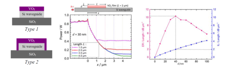
Figure 1: (a, figure on the left) Schematic cross-section of two designs of the photonic waveguide switch; (b, figure in the middle) FEM simulation of power transmission through a photonic waveguide switch of type 1 in metallic state for the TE mode at 1550 nm. The length L and thickness d of the VO2 film structure are indicated; (c, figure on the right) simulated extinction ratio ER and insertion loss IL of the TE mode at 1550 nm versus VO2 film thickness d (type 2).
The following figure shows a SEM micrograph of a photonic waveguide switch of type 2. We use the fabrication technology comprising of a two-step e-beam lithography (EBL) and etching processes. In the first EBL step, the patterns of waveguides and grating couplers are transferred to the Si device layer of a silicon-on-insulator (SOI) chip. Si is etched anisotropically using a cryogenic RIE process. The second EBL step is used to define the local openings for VO2 deposition. After lift-off, samples are post-annealed at 550 °C [1].
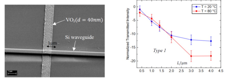
Figure 2: Figure on the left: SEM picture of a photonic waveguide switch of type 2. Length and width of VO2 film structure on top of the waveguide are 1 μm and 0.5 μm respectively. Figure on the right: Normalized optical transmission of the TE mode at 1550 nm as a function of VO2 film length L at substrate temperatures of 20 and 80 °C.
Publication List
- Li, Z.; Rastjoo, S.; Ewy, A.; Wang, X.; Ludwig, A.; Kohl, M. Design and Fabrication of a Photonic Waveguide Switch Based on a VO2 Film. International Conference on Micro- and Nano Engineering (MNE), Turin, Italy, 2021.
- Rastjoo, S.; Wang, X.; Ludwig, A.; Kohl M. Top-down fabrication and transformation properties of vanadium dioxide nanostructures. J. Appl. Phys. 2019; 125 (22): 225104.
- Rastjoo, S.; Wang, X.; Ludwig, A.; Kohl M. Fabrication and Transformation Properties of Vanadium Dioxide Bimorph Nanoactuators. Shape Memory and Superelastic Technology Conference and Exposition (SMST), Konstanz, Germany, 2019.
- Rastjoo, S. (2020). Development of Nanodevices Based on VO₂ Thin Films. Dissertation, Karlsruher Institut für Technologie (KIT), Fakultät für Maschinenbau (MACH), DOI: 10.5445/IR/1000120274.
Funding/ Projects
DFG Project: VO2nano